Silicon
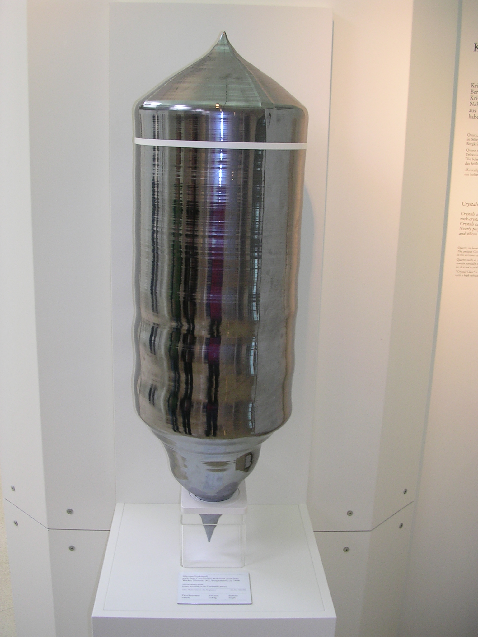

Silicon is the material on which the whole of electronics rests — and in neutrinovoltaic technology it forms one half of the layer stack, the other half of which is graphene.
The second most abundant element in the Earth's crust
After oxygen, silicon is at around 28 percent the most common constituent of the Earth's crust. It is in ordinary sand, in quartz, in almost every rock.
In nature, however, it never occurs pure. The path from sand to semiconductor crystal is one of the most elaborate in industry: reduction in an electric arc furnace, purification via trichlorosilane, finally the pulling of a single crystal by the Czochralski process. Microelectronics demands a purity of 99.9999999 percent — at most one foreign atom per billion silicon atoms.
Why silicon of all things
The reason is the band gap. In a solid, electrons may take only certain energies; between the filled valence band and the empty conduction band a semiconductor has a gap. In silicon it amounts to 1.12 electronvolts.
This value is happily chosen — not by people but by nature. It is large enough that thermal motion at room temperature does not constantly lift electrons across, and small enough that this can be done deliberately: by light, by an electric field, by introduced foreign atoms.
Transistor, solar cell and image sensor all rest on exactly this.
Doping
Introducing foreign atoms into the crystal lattice changes the behaviour fundamentally.
Phosphorus has one outer electron more than silicon. The surplus electron finds no bonding partner and becomes mobile — this is called n-doping.
Boron has one fewer. A vacancy arises that behaves like a positive charge — p-doping.
Bringing both regions together creates a p-n junction, and that lets current through in one direction only. This rectification is the core of all semiconductor technology — and it is also the point at which neutrinovoltaic technology begins.
Silicon in neutrinovoltaic technology
Patent WO2016142056A1 describes a film on which graphene and silicon are deposited alternately — ten to twenty layers, twelve in particular. The silicon fraction is given as 10 to 80 percent, 25 percent being especially preferred. The particle size is to lie between 5 and 500 nanometres.
That size specification is the interesting part. Silicon in the nanometre range behaves differently from a bulk crystal: the band gap shifts, the ratio of surface to volume becomes very large, and interfaces gain importance relative to the interior.
The role assigned to silicon in the group's account is that of the conducting medium: it takes up the motion generated in the graphene lattice and passes it on to the carrier material. Graphene supplies the structure, silicon the path for the charge.
The difference from a solar cell
A solar cell uses silicon as well, but differently. There an incoming photon lifts an electron across the band gap; without light nothing happens. The cell is a surface, and its yield grows with that surface.
The master equation of neutrinovoltaic technology, by contrast, integrates over the volume. The yield is therefore meant to grow with the number of layers, not with the illuminated area.
Other uses
Silicon is also the material of many neutrino detectors. Semiconductor detectors of ultra-pure silicon or germanium measure energies very precisely — they stand behind the search for neutrinoless double beta decay and behind the small detectors for coherent scattering off atomic nuclei.
The same element thus appears on both sides of this wiki: as a tool for measuring neutrinos, and as a building material in the attempt to win energy from them.
Related
- Graphene — the other half of the layer stack
- Doped graphene — the tuned variant
- Patent WO2016142056A1 — the quantities specified
Sources
- WIPO: WO 2016/142056 A1, claims on composition and particle size.
- Neutrino® Energy Group: Neutrinovoltaic, neutrino-energy.com.